High-Power Electronics
Electric Vehicles are Driving the Demand for SiC Wafers for High Power Electronics
Silicon Carbide (SiC) power electronics provide higher power density and higher efficiency than silicon-based technologies, enabling faster charging times and expanded EV range.


Enabling Clean Technologies with WBG Semiconductors for the Promise of a More Sustainable Future
As the focus on decarbonizing the world and meeting environmental goals has become a central priority for global regulators and manufacturers alike, the need to deploy greener and more environmentally sustainable solutions continues to expand. Electrifying the transportation sector is critical to the global clean energy transition. The application of wide bandgap (WBG) devices in electric vehicles (EVs) and charging stations is driving the growth of the WBG market because of their higher efficiency, high thermal conductivity, higher breakdown voltage and higher power density. With their ability to withstand higher electric fields, voltages, frequencies, and temperatures than their silicon-based predecessors, silicon carbide (SiC) and gallium nitride (GaN) WBG semiconductor power device market will continue to rapidly expand.


WBG Semiconductor Device Applications
Applications for WBG circuits within the transportation sector include the electrification of trains, ships, and aircraft. Renewable energy applications such as solar photovoltaics and wind energy will benefit from SiC and GaN circuitry by minimizing conversion losses and increasing overall energy efficiency. These WBG semiconductors are also expected to impact the telecommunications market including 5G wireless devices as they enable smaller, lighter circuits that can withstand higher voltages with less thermal restriction.

EV Auto Industry Driving the Demand for WBG Semiconductor Devices
The Electric Vehicle (EV) Industry is driving the transition from silicon-based power electronics to silicon carbide (SiC) and gallium nitride (GaN) wide bandgap (WBG) semiconductors. In particular, SiC power devices including metal–oxide–semiconductor field-effect transistors (MOSFETs), Schottky barrier diodes, and power modules have displaced silicon-based devices in EV drivetrains due to overall size, reliability, and energy efficiency. Demand for silicon carbide power devices is tracking the exponential growth of the EV industry.
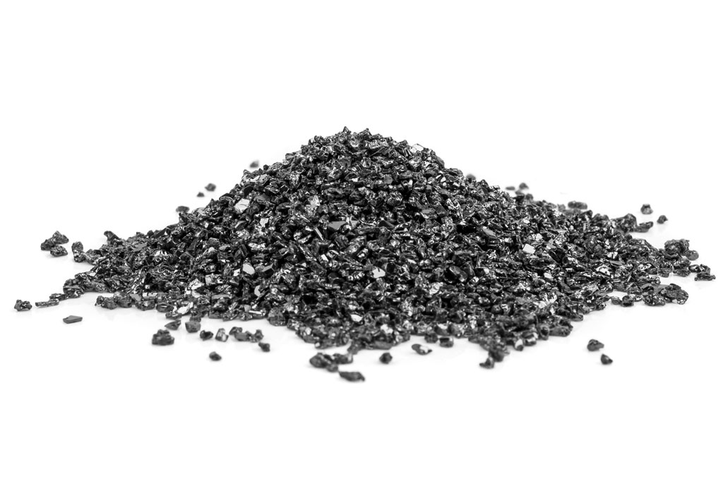
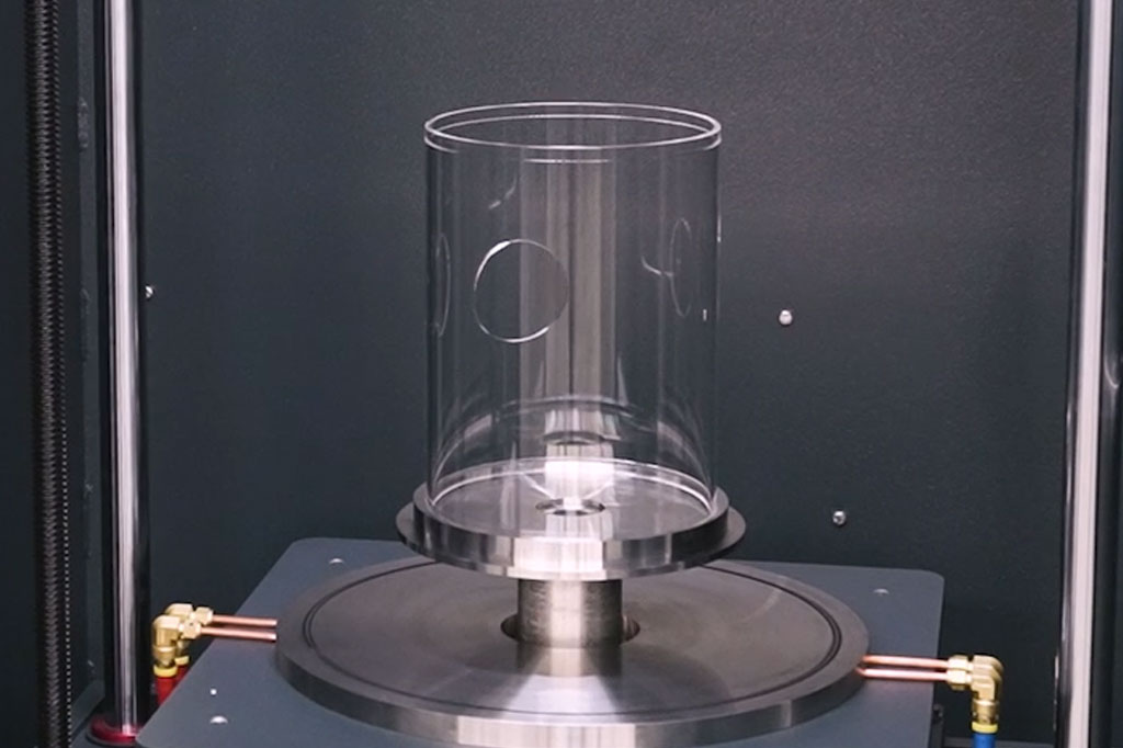
Physical Vapor Transport Process for Silicon Carbide Crystal Growth
Physical Vapor Transport (PVT) is the most advanced crystal growth method available today. In this process, polycrystalline silicon carbide (SiC) source material undergoes sublimation at high temperatures of up to 2,500°C and low pressures. Thermodynamics and chemical kinetics drive the reaction. During PVT processing, the growth rate is controlled by the mass transport of reactants to the seed crystal growth surface for diffusion-controlled growth. These processes often run for days and sometimes weeks at a time; system process controls are critical to the quality of low defect crystal growth for 150 mm and 200 mm boule diameters.
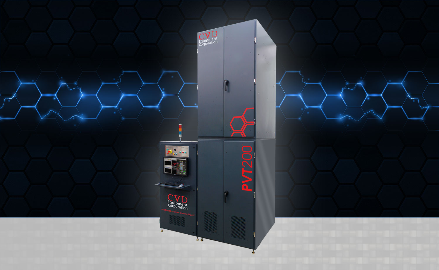

CVDE’s Industrial Physical Vapor Transport Systems for Silicon Carbide Crystal Growth
These systems are used to grow various crystals such as silicon carbide (SiC) and aluminum nitride (AlN) which are subsequently processed into wafers to support high-power electronics applications. The demand for SiC boules / ingots and epi-ready wafers continues to accelerate for electric vehicles, energy, and industrial applications. Our PVT product series provides precise and reliable control of all process parameters. This allows for high yield, run-to-run repeatability, and system-to-system matching. The required high temperatures are achieved with an RF induction heating system. The automated positionable coil with axial vertical travel allows for the control of thermal gradients and optimizes SiC growth.
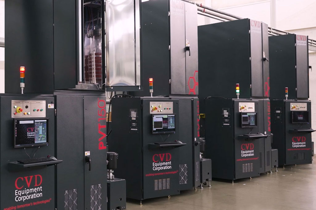
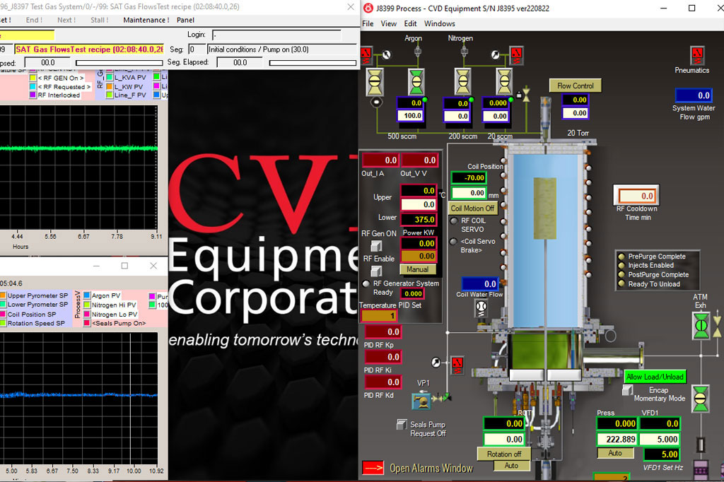
CVDE’s Leadership Role in Manufacturing High-Performance Process Equipment
CVD Equipment manufactures the highest quality silicon carbide and gallium nitride-related production systems for the compound semiconductor industry. Leveraging over 40 years of knowledge in chemical, electrical, and process equipment engineering built into our systems. Supplying Physical Vapor Transport, Annealing, Epitaxial Growth, and Hydride Vapor Phase Epitaxy Systems to manufacturers and leading research and academic institutions, our highly engineered equipment delivers the technology that will build tomorrow’s high-powered electric future.

Polycrystalline SiC + Argon Gas
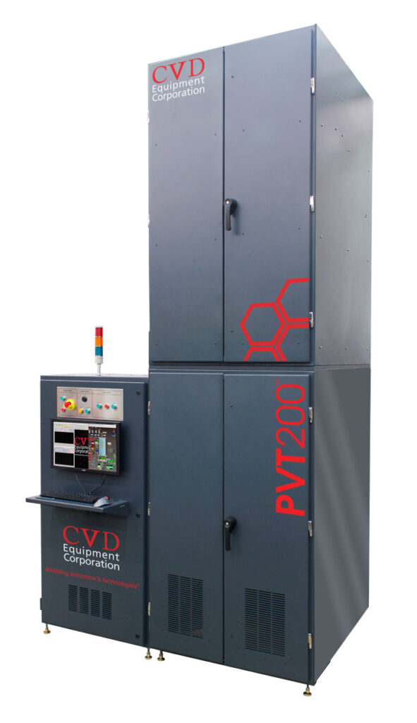
CVD Equipment’s PVT Processing Systems
High-Quality SiC Crystal Boules
CVD Equipment Corporation introduces state-of-the are physical vapor transport (PVT) systems for silicon carbide (SiC) crystal boule growth. With precise thermodynamics and chemical kinetics to drive the reaction, polycrystalline SiC will sublime under low pressure and high temperatures. Our PVT product series provides precise and reliable control of all process parameters. Exclusively engineered for high yield, run-to-run repeatability and system-to-system matching, 150 mm and 200 mm boule diameters can be achieved.
PVT System Features & Benefits:
Physical Vapor Transport (PVT) systems for the growth of 150 & 200+ mm diameter single crystal boules
Crystal Growth & Annealing
Robust Production System with Enhanced Process Controls
– Temperature Control +/- 0.5°C
– Pressure Control +/- 1%
High Temperature, RF Induction Heating up to 2500°C
Standard and Custom Coil Designs
Custom Quartzware
Automatic Crucible Load/Unload and Recipe Start
Crucible Stage Rotation supports accelerated production needs/critical high-volume manufacturing
Automated Repositionable RF Coil with axial vertical travel allows for the control of thermal gradients and optimizes SiC growth.
Motorized Pyrometer Alignment via Remote Control Box for real-time monitoring of crystal growth
Vacuum System with Atmospheric Bypass
Manufacturing Enterprise System (MES) Compatible Integration
Compact Manufacturing Footprint
Hydride Vapor Phase Epitaxy (HVPE) Systems are used to grow polycrystalline bulk gallium nitride (GaN) as the precursor for monocrystalline gallium nitride wafer production. Our HVPE systems are also used to grow thick epitaxial single crystal layers of doped and undoped gallium nitride, Aluminum Nitride (AlN), Gallium Arsenide (GaAs), Indium Phosphide (InP), and other binary and ternary systems where a metal halide is reacted with one or several hydrides to form a solid crystal. CVDE understands the needs of our customer base and prides itself on the wide array of system features and options we can offer; this sets us apart from other OEMs. We’ve artfully engineered so you can deliver better results.
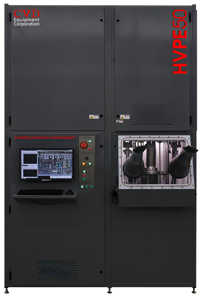
HVPE System Features & Benefits:
Configured for Optimal Growth Parameters/Conditions for a Range of Doped and Undoped III/V Epitaxial Crystals, Including GaN, GaAs, AlN, InP, etc.
Dual Chamber Design for Abrupt Multilayer Deposition Available
Multi-zone Furnace (Resistive or RF Induction Heated)
Vertical Process Tube with Pre-Chambers for Chlorination
Chlorination Chambers for Dopant Chlorides are Available
Substrate Rotation for Improved Deposition Uniformity
Loading Station with Optional Nitrogen-Purged Glovebox
Optional Gas Delivery Cabinets
Optional Exhaust Gas Emission Treatment
State-of-the-art Safety Enhancement Control Measures
CVDWinPrC™ System Control Software for Real-Time Process Control, Data Logging, and Process Recipe Editing
Designed to Accommodate the End User’s Configuration Requirements
About Us
Over 40 years of expertise in CVD and thermal process equipment design and manufacturing.
“enabling tomorrow’s technologies ™ ”
