Nanomaterials and Semiconductors
Nanomaterials & Semiconductors
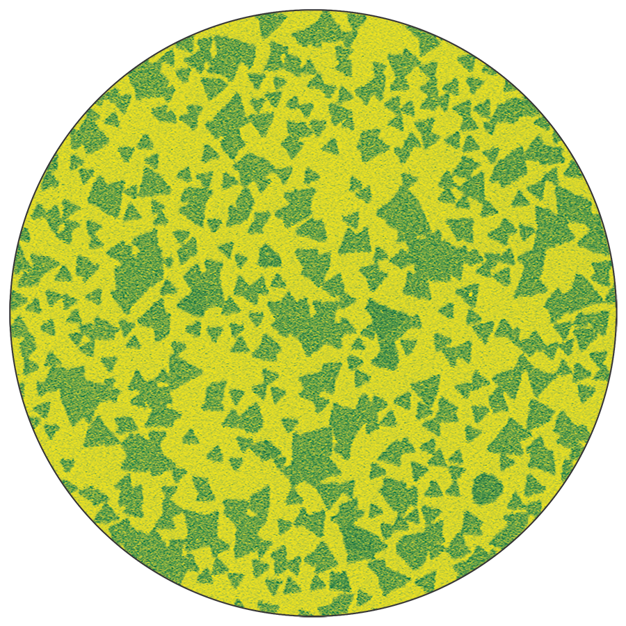
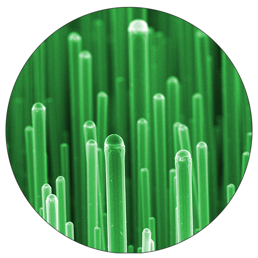
FirstNano® R&D systems for processing graphene, carbon nanotubes, semiconducting nanowires, 2D materials, and thin films for research laboratories. CVD process equipment is used in the fabrication of solar cells and TCO coatings as well as semiconductors and optoelectronics materials.
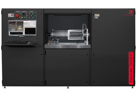
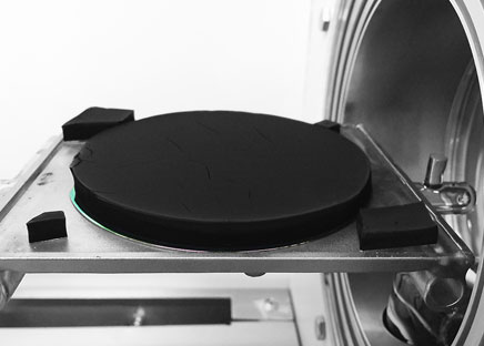
CVD Equipment is the Leading Supplier of Nanomaterials Synthesis Systems
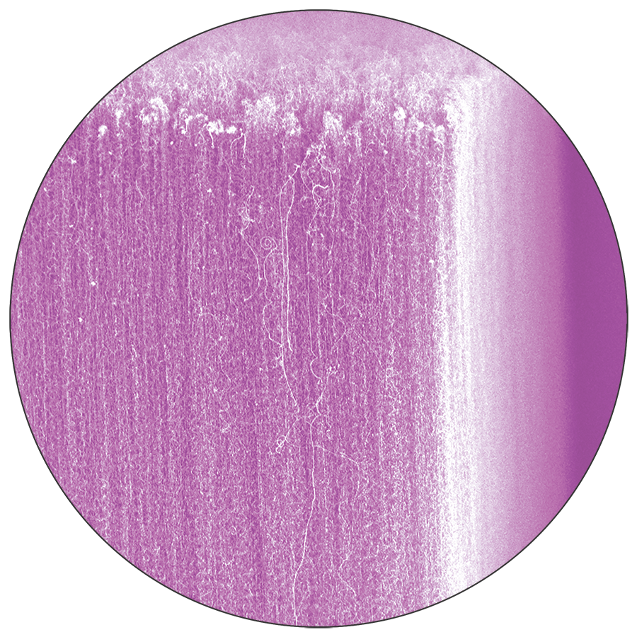
Our FirstNano® division has supplied hundreds of EasyTube® systems worldwide. We work closely with our customers in continuously developing cutting-edge equipment and processes for Carbon Nanotubes (CNTs), Nanowires, Graphene, 2D materials and emerging technologies. We also developed and manufacture a Carbon+ 300™ pilot production system to support our industrial customers in commercializing high-quality carbon nanomaterials.

Chemical Vapor Deposition for the Semiconductor Industry
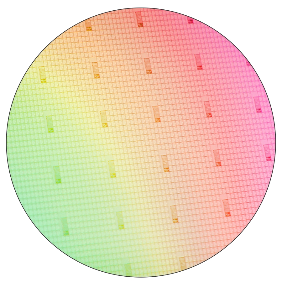
Crystalline compound semiconducting materials form the foundation of many devices that are widely used in everyday life, including complementary metal-oxide-semiconductor (CMOS) integrated circuits (ICs), optoelectronic and photonic devices, and micro-electro-mechanical systems (MEMS). Chemical vapor deposition (CVD) is the most widely adopted industrial technique for producing semiconducting thin films and complex layered micro- and nanostructures. The CVD process is versatile and can be tuned to produce homoepitaxial and heteroepitaxial monocrystalline materials as well as polycrystalline and amorphous materials. A high level of dopant control can be readily achieved for fine-tuning the electronic properties.
Common semiconducting materials include silicon, germanium, arsenic, antimony, etc. They can be formed in binary, ternary, and Quaternary compounds with metals such as aluminum, gallium, and indium. They are also generated in the form of oxides, nitrides, carbides, etc. Each semiconducting material or compound has specific properties that can be exploited to realize a particular device. Common semiconducting thin films include silicon carbide (SiC), gallium nitride (GaN), gallium arsenide (GaAs), etc. Complex structures such as multi-layer stacks, nanowires/nanorods, and quantum dots can be produced using CVD processes.
For more information on the Silicon Carbide Semiconductor market click the button below.
CVD Equipment Corporation has over 40 years of experience in designing and manufacturing turn-key CVD systems. Our products meet the stringent demands required in order to maintain controllable and repeatable deposition of high quality, high purity semiconducting crystal structures, and epitaxial layers. We have developed a modular platform that allows user to configure their equipment for their specific requirements. Our technology is tried and tested, with systems in operation worldwide.
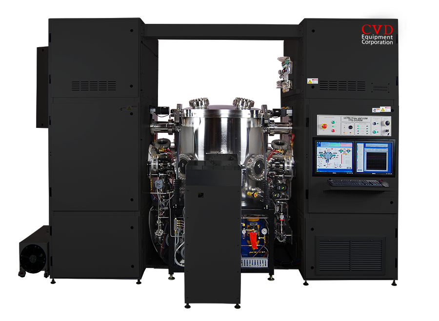
UHVCVD System Features & Benefits:
Manufacturing Enterprise System (MES) Compatible Integration
CVDWinPrC™ system control software for real-time process control, graphing, data logging, and process recipe editing
Robust, low-maintenance design

About Optoelectronics Materials Production Equipment
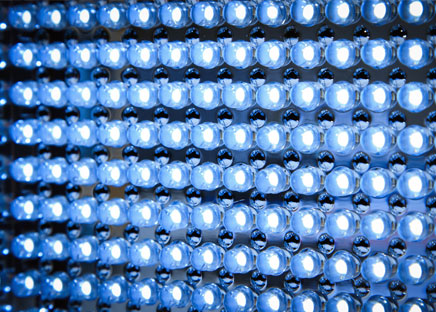
Semiconductor materials are widely used in optoelectronics devices such as light-emitting diodes (LEDs) and infrared detectors. Light Emitting Diodes: Blue LEDs used in white light applications are typically made from gallium nitride and its ternary alloys with indium, aluminum, etc. New materials such as ZnO and ZnSe are currently being studied for the next generation of LEDs. Infrared Detector: HgCdTe (mercury cadmium telluride, MCT) is the most commonly used material for infrared detectors.
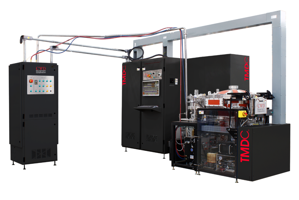
MOCVD System Features & Benefits:
Horizontal or Vertical process chamber
Wafer size is configurable to meet the requirements of end-user
Resistance, IR, or RF heated depending on the temperature requirements
Temperature controlled showerhead
Wafer rotation
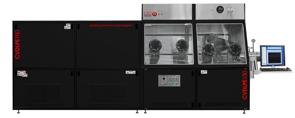
LPECVD System Features & Benefits:
Multi-zone rolling resistance furnace for temperatures up to 700°C
+/- 0.25°C temperature uniformity over the flat zone
Rapid controlled heat-up and cool-down of LPE boat
Automatic boat slider

About CVD Deposition Equipment for Solar Photovoltaics
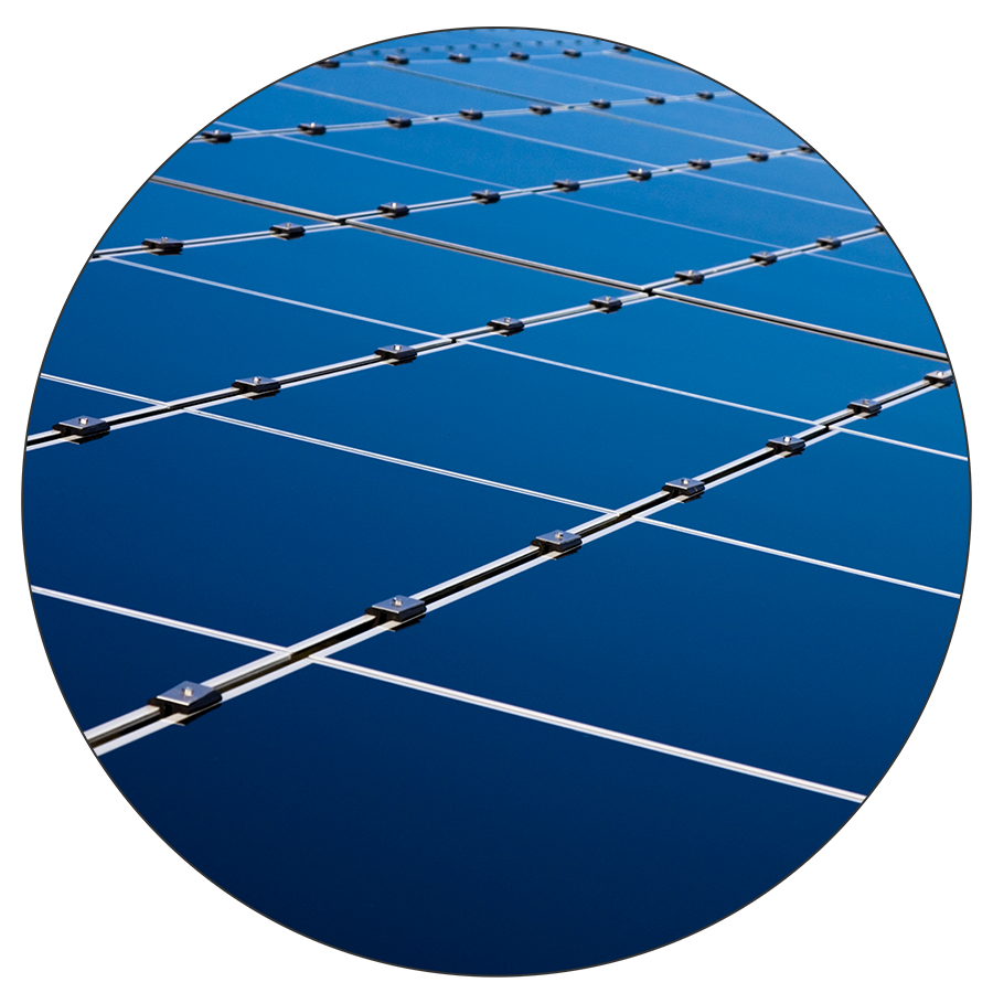
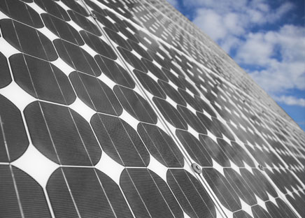
CVD Equipment Corporation provides key process equipment used in the fabrication of solar cells. Our equipment is used for steps including diffusion, deposition of antireflective layers, oxidation, and silicon epitaxial deposition. Additionally, we provide our application laboratory services, for research laboratories and companies, to support their efforts for improving solar cell functionality, properties, and efficiency. We supply CVD production equipment for use in large-scale solar cell manufacturing, with a low cost-of-ownership (COO).
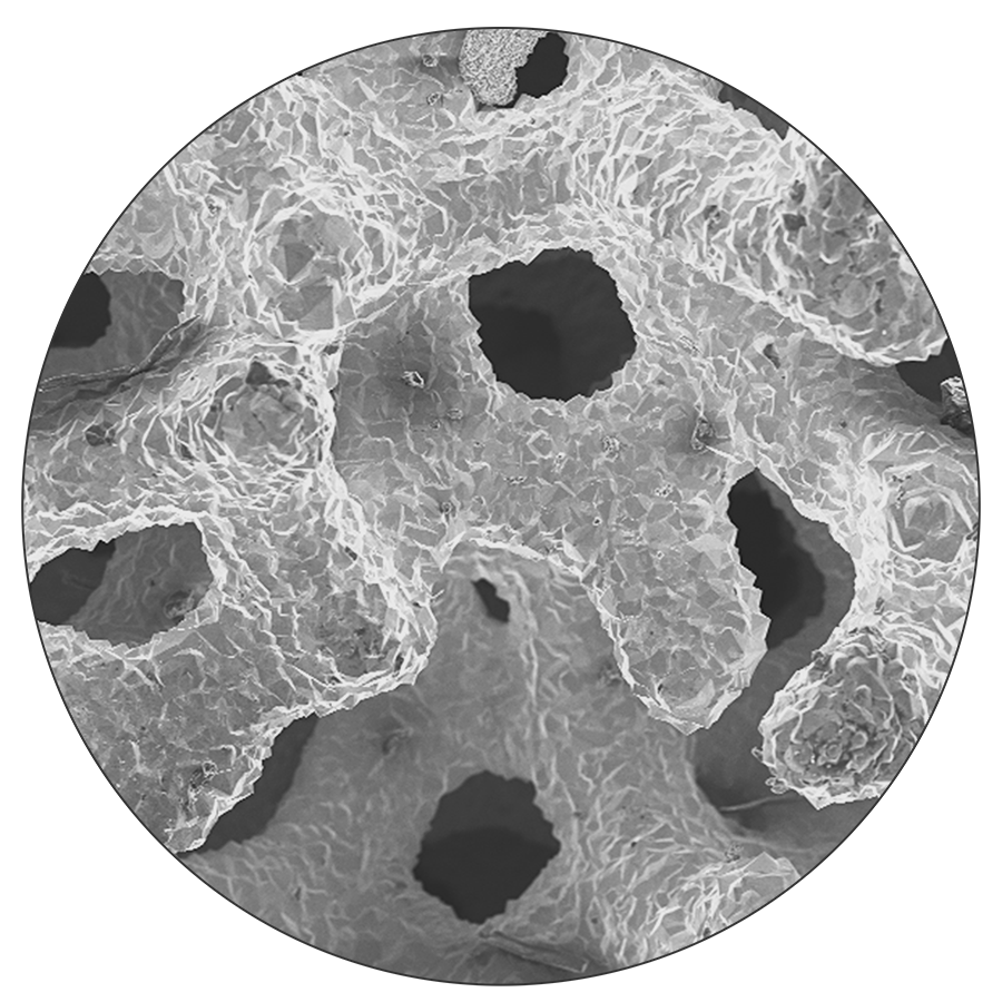
CVD processes are widely used in solar cell manufacturing, from the deposition of crystalline silicon in a c-Si solar cell, to the deposition of a range of different materials in thin film solar cells (TFSCs). Other examples of uses of CVD Equipment Corporation’s CVD processing equipment in the solar industry include deposition of amorphous silicon (a-Si), micro-crystalline silicon (μc-Si), silicon, silicon-germanium, etc. Also, our equipment is used for trichlorosilane (TCS) source quality control, antireflection (AR) coatings such as silicon nitride and high or low temperature silicon dioxide, transparent conductive oxides (SnO2, ZnO, etc.), sulfurization/selenization, rapid thermal annealing, doping (e.g. using phosphoryl chloride, POCl3) and other related dopant diffusion processes needed for next generation silicon and copper-indium-gallium-selenide (CIGS) solar cell modules.
Si wafer based Solar Cell
Diffusion
Oxidation
Si based Thin Film Solar Cell
a-Si and μc-Si Deposition
Chemical Compound based Thin Film Solar Cell
Selenization and Sulfurization
Multi-junction Photovoltaic Cell
Antireflection Coating
Antireflection Coating
TCO Coating
Silane and Chlorosilane Precursor Quality Control
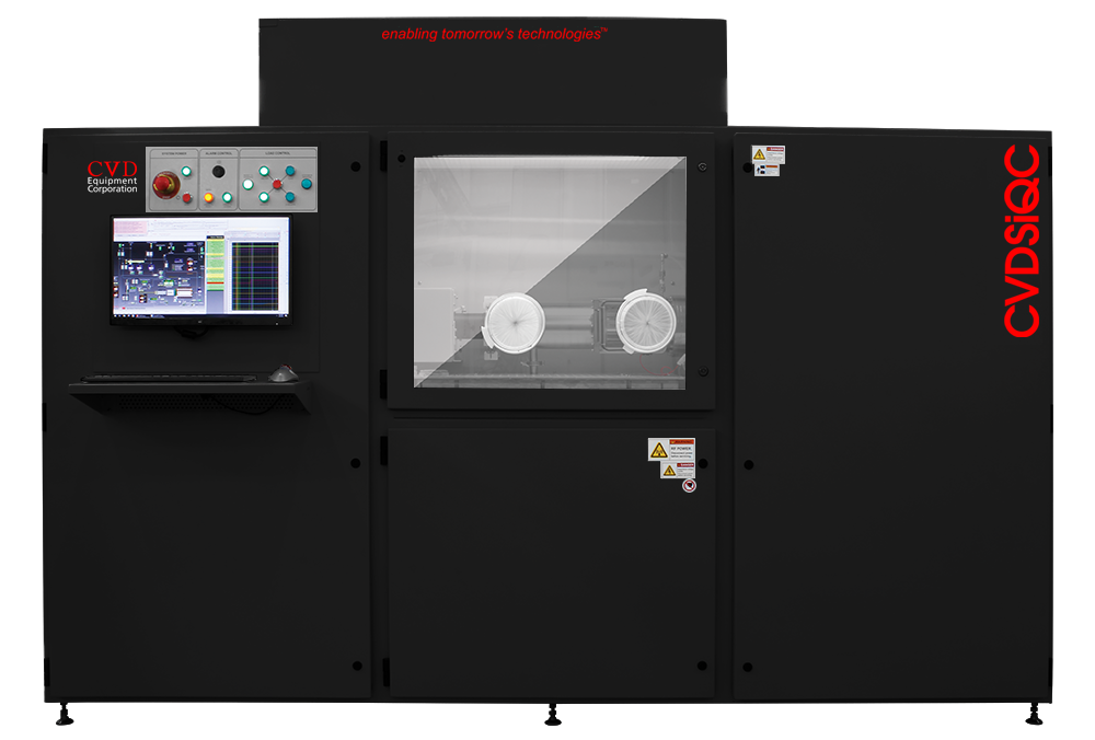
SiQC System Features & Benefits:
Preprogrammed Recipes for Silicon Epitaxial Deposition
Processes up to two float zone wafers per run
High purity susceptor
Cantilevered automatic substrate loading/unloading system
Loadlock isolates the process tube from ambient atmosphere during loading and unloading


About Transparent Conductive Oxide Coatings
Transparent conductive oxide (TCO) coatings are key in large-scale thin film solar cell manufacturing. CVD Equipment Corporation provides online and offline atmospheric-pressure chemical vapor deposition processing equipment for fluorine-doped tin oxide (SnO2:F or FTO) coatings and offline low-pressure chemical vapor deposition processing equipment for boron doped zinc oxide (ZnO:B) coatings. TCOs can be coated on soda lime glass sheets and on a wide variety of metal foils and plastics. They can be optimized for rough coating with high haze for solar applications and with low haze for Low-E and other smart glass applications. Fluorine-doped zinc oxide has the potential to have 4X better performance for solar applications than boron-doped zinc oxide but requires higher deposition temperatures.
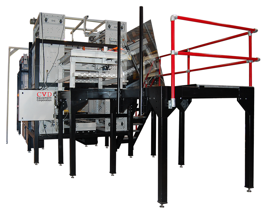
APCVD System Features & Benefits:
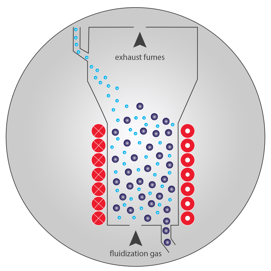
Deposit a layer of material onto wafers or other types of substrates
Grow epitaxial films of Si, compound semiconductors, SiO2, anti-reflection (AR) coatings, and transparent conductive oxide (TCO) coatings
Surface-finishing process for items such as tools and turbine blades to improve lifetime and performance
About Us
Over 40 years of expertise in CVD and thermal process equipment design and manufacturing.
“enabling tomorrow’s technologies ™ ”
